The following items are available in stock.
Call 1-858-876-3133 for availability or email us to place your order while supplies last! Do not see waht you want in the list? E-mail for a custom quote!
Cadmium selenide (CdSe) is a solid,
binary compound of cadmium and selenium. Common names for this compound are
cadmium(II) selenide, cadmium selenide, and cadmoselite (a very rare mineral).
Cadmium selenide is a semiconducting material, but has yet to find many
applications in manufacturing. This material is transparent to infra-red (IR)
light, and has seen limited use in windows for instruments utilizing IR light.
Much current research on cadmium selenide has focused on nanoparticles.
Researchers are concentrating on developing controlled syntheses of CdSe
nanoparticles. In addition to synthesis, scientists are working to understand
the properties of cadmium selenide, as well as apply these materials in useful
ways. (Wikipedia)
1 CdSe powder 10-30 um (within 1 batch), 99.999 %, 10 kg.
2 CdSe, 6 X 4 X 2 mm, 6 X 4 // (0001), all sides polished 60/40, high
resistivity (>/= 10^11 Ohm*cm), 11 pcs.
3 CdSe, random oriented, 10 X 10 X 0.5mm, 2 sides polished 60/40, high
resistivity (>/= 10^11 Ohm*cm), 1 pc.
4 CdSe (10-10), 25X15X1 mm, 2 sides polished 60/40, low resistivity (< 1
Ohm*cm), 2 pc.
5 CdSe, Dia: 12.7 X 3.2 mm, <0001> // Dia: 12.7, 2 sides polished 60/40, high
resistivity (>/= 10^11 Ohm*cm), 1 pc.
6 CdSe,Dia: 10 X 0.3 mm, // "c", polished 60/40, 5 pcs.
7 CdSe, 5X5X0.5 mm, (0001), all sides polished 60/40, high resistivity (>/=
10^11 Ohm*cm), 5 pcs.
8 CdSe, (0001), 10 X 10 X 0.5 mm, 1 side polished 60/40, 1 side grinded, low
resistivity (< 1 Ohm*cm), 7 pcs.
9 CdSe, // "c", 10 X 10 X 1 mm, 2 sides polished 60/40, low resistivity (< 1
Ohm*cm), 5 pcs.
10 CdSe Dia: 5 X 5 mm, (0001), 2 sides polished 60/40. High resistivity (>/=
10^11 Ohm*cm), 4 pcs.
11 CdSe, 5 X 5 X 1 mm, (0001), all sides polished 60/40, low resistivity(< 1
Ohm*cm), 10 pcs.
12 CdSe, random oriented, 10 X 10 X 0.5 mm, 2 sides polished 60/40, low
resistivity (< 1 Ohm*cm), 9 pcs.
1 CdTe (110), 10 X 8 X 3 mm, 2 sides polished 60/40, high resistivity (>/= 10^6
Ohm*cm), n-type, 1 pc.
2 CdTe, 5 X 5 X 1.3 mm, (110) at 45deg to 5 X 5 mm, 2 sides polished 60/40, high
resistivity (>/= 10^6 Ohm*cm), 7 pcs.
3 CdTe, 6 X 4 X 2 mm, 6 X 4 // (111), all sides polished 60/40, high resistivity
(>/= 10^6 Ohm*cm), 8 pcs.
4 CdTe, Dia: 6 X 8 mm, Dia: 6 //(111), high resistivity (>/= 10^6 Ohm*cm), 2
pcs.
5 CdTe, Dia: 15 X 2 mm, (110), 2 sides polished 60/40, high resistivity (>/=
10^6 Ohm*cm), 3 pcs.
6 CdTe, 10 X 10 X 1 mm, random oriented, 2 sides inspection polished, high
resistivity (>/= 10^6 Ohm*cm), 4 pcs.
7 CdTe, 7 X 5 X 0.5 mm, (110), 3 sides polished 60/40, high resistivity(>/= 10^6
Ohm*cm), 5 pcs.
8 CdTe, 30 X 2 X 1 mm, 30 X 2 // (110), 2 sides polished 60/40, high resistivity
(>/= 10^6 Ohm*cm), 3 pcs.
9 CdTe, Dia: 27 X 1.5 mm, (111), 2 sides polished 60/40, high resistivity (>/=
10^6 Ohm*cm),1 pc.
10 CdTe, 30 X 3 X 3 mm, 30 X 3 // (111), 3 X 3 // (110), all sp 60/40, high
resistivity (>/= 10^6 Ohm*cm), 2 pcs.
11 CdTe, 10 X 10 X 0.5 mm, (110), 1 side polished 60/40, 1 side fine grinded,
low resistivity, p-type, 2 pcs.
12 CdTe, 10 X 10 X 0.2 mm, (110), 2 sides polished 60/40, high resistivity (>/=
10^6 Ohm*cm), 1 pc.
13 CdTe, 10 X 5 X 1 mm, (110), 2 sides polished 60/40, high resistivity(>/= 10^6
Ohm*cm), 1 pc.
14 CdTe, 5 X 5 X 2 mm, (110), 2 sides polished 60/40, high resistivity (>/= 10^6
Ohm*cm), 1 pc.
15 CdTe, 10 X 10 X 2 mm, (110)/(110)/(100), 2 sides polished 60/40, high
resistivity (>/= 10^6 Ohm*cm), 1 pcs.
16 CdTe, 10 X 10 X 0.5 mm, (100), 1 side polished 60/40, 1 side fine grinded,
p-type, 3 pcs.
17 CdTe, 10 X 10 X 0.5 mm, random oriented, 1 side polished 60/40, 1 side fine
grinded, p-type, 7 pcs.
18 CdTe, 10 X 10 X 0.5 mm, (100), 2 sides polished 60/40, p-type, 2 pcs.
19 CdTe, 10 X 10 X 0.5 mm, (110), 2 sides polished 60/40, high resistivity (>/=
10^6 Ohm*cm), 1 pc.
20 CdTe, 10 X 10 X 0.5 mm, (111), 2 sides polished 60/40, high resistivity (>/=
10^6 Ohm*cm), 1 pc.
21 CdTe, 10 X 10 X 1 mm, (100), 2 sides polished 60/40, high resistivity (>/=
10^6 Ohm*cm), 4 pcs.
22 CdTe, 20 X 20 X 1 mm, (110), 2 sides polished 40/20, high resistivity (>/=
10^6 Ohm*cm), 1 pc.
1 ZnTe 10 x 10 x 0.5 mm, (110), 2 sides polished 60/40, 3pcs.
2 ZnTe 10 x 8 x 0.8 mm, (110), 2 sides polished 60/40, 2pcs.
3 ZnTe 10 x 8 x 0.2 mm, (110), 2 sides polished 60/40, 1pc.
4. ZnTe 10 x 8 x 1 mm, (110), 2 sides polished 60/40, 2pcs.
5. ZnTe 10 x 10 x 0.4 mm, (110), 2 sides polished 60/40, 1pc.
Call 1-858-876-3133 for availability or email us to place your order while supplies last! Do not see waht you want in the list? E-mail for a custom quote!
References
Lev Isaakovich Berger (1996). Semiconductor materials. CRC Press. p. 202. ISBN
0849389127.
II-VI compound crystal growth, HPVB & HPVZM basics
a b Didenko, Yt; Suslick, Ks (Sep 2005). "Chemical aerosol flow synthesis of
semiconductor nanoparticles.". Journal of the American Chemical Society 127
(35): 12196–7. doi:10.1021/ja054124t. ISSN 0002-7863. PMID 16131177.
Murray, C. B.; Norris, D. J.; Bawendi, M. G. (1993). "Synthesis and
characterization of nearly monodisperse CdE (E = sulfur, selenium, tellurium)
semiconductor nanocrystallites". Journal of the American Chemical Society 115:
8706. doi:10.1021/ja00072a025.
T Ohtsuka, J Kawamata, Z Zhu, T Yao (1994). "p-type CdSe grown by molecular beam
epitaxy using a nitrogen plasma source". Applied Physics Letters 65: 466.
doi:10.1063/1.112338.
Ma, C; Ding, Y; Moore, D; Wang, X; Wang, Zl (Jan 2004). "Single-crystal CdSe
nanosaws.". Journal of the American Chemical Society 126 (3): 708–9.
doi:10.1021/ja0395644. ISSN 0002-7863. PMID 14733532.
Califano, Marco; Zunger, Alex; Franceschetti, Alberto (2004). "Direct carrier
multiplication due to inverse Auger scattering in CdSe quantum dots". Applied
Physics Letters 84: 2409. doi:10.1063/1.1690104.
Schaller, Richard D.; Petruska, Melissa A.; Klimov, Victor I. (2005). "Effect of
electronic structure on carrier multiplication efficiency: Comparative study of
PbSe and CdSe nanocrystals". Applied Physics Letters 87: 253102.
doi:10.1063/1.2142092.
Hendry, E.; Koeberg, M; Wang, F; Zhang, H; De Mello Donegá, C; Vanmaekelbergh,
D; Bonn, M (2006). "Direct Observation of Electron-to-Hole Energy Transfer in
CdSe Quantum Dots". Physical Review Letters 96 (5): 057408.
doi:10.1103/PhysRevLett.96.057408. PMID 16486988.
Nanotechnology Structures - Quantum Confinement
Colvin, V. L.; Schlamp, M. C.; Alivisatos, A. P. (1994). "Light-emitting diodes
made from cadmium selenide nanocrystals and a semiconducting polymer". Nature
370: 354. doi:10.1038/370354a0.
Chan, W. C.; Nie, S. M. (1998). "Quantum Dot Bioconjugates for Ultrasensitive
Nonisotopic Detection". Science 281: 2016. doi:10.1126/science.281.5385.2016.
Bruchez, M.;Moronne, M.; Gin, P.; Weiss, S.; Alivisatos, A. P. (1998). Science
281: 2013.
[PDF] Preparation and Characterization
of CdSe Single Crystal
by A Abd-El Mongy - Related articles
High quality of CdSe single crystal is grown from the melt. X-ray ... For CdSe
crystal growth, the starting material was bought with labeled ...
Cadmium selenide - Wikipedia, the free encyclopedia
Cadmium selenide in its wurtzite crystal structure is an important II-VI
semiconductor. As a semiconductor CdSe is an n-type semiconductor, ...
A tunable infrared parametric oscillator in a CdSe crystal - Elsevier
by AA Davydov - 1973 - Cited by 23 - Related articles
We have demonstrated an infrared singly resonant parametric tunable oscillator
in a CdSe crystal. The oscillator was pumped at 2.36 μ (CaF2: Dy2+ laser) and
...
Cadmium selenide (CdSe) crystal structure, modifications
Cadmium selenide (CdSe) crystal structure, modifications. Madelung, O., Rössler,
U., Schulz, M. (ed.). SpringerMaterials - The Landolt-Börnstein Database ...
Efficient cw lasing in a Cr2+:CdSe crystal
by VA Akimov - 2007 - Cited by 1 - Related articles
beam was focused on the Cr2‡ :CdSe crystal by spherical ... lasing in a Cr2‡
:CdSe crystal at 2.623 mm. The half-width of the laser spectrum was about 10 nm
...
Efficient cw lasing in a Cr2+:CdSe crystal
by VA Akimov - 2007 - Cited by 1 - Related articles
Aug 10, 2010 ... Continuous wave lasing in a Cr2á : CdSe crystal is obtained for
the first time. ... The Cr2á : CdSe crystal was pumped through mirror M1 ...
SANS Study of CdS and CdSe Quantum Dot Crystal Growth in a Silica ...
by N De La Rosa-Fox - 1998 - Cited by 2 - Related articles
CdS and CdSe crystal growth as quantum dots using small-angle neutron scattering
techniques (SANS). Thus, the crystal growth influences the aggregation ...
Optical properties of transition metal impurities in CdSe. I ...
by JM Langer - 1971 - Cited by 30 - Related articles
in CdSe crystals are presented. The main features of the spectra are
successfully inter- pret,ed using crystal-field theory for the states of 3dn ...
[PDF] No Job Name
Oct 19, 2004 ... the top of the CdSe crystal (Figure 1c), indicating the equal
growth rate of all the nanowires. This result also shows that the ZnS ...
Single-crystal CdSe nanosaws.
We report the first successful synthesis and characterization of single-crystal
wurtzite CdSe nanoribbons through a simple thermal evaporation process. ...
Optics from A to Z -
Greyhawk_links
Axicons (doc
- pdf)
buy online -
BaF2 optics -
buy online -
LiF optics -
LiF VUV-
buy online -
Ge optics -
buy online -
Dimond-like
carbon coating
Hollow Beam
Atom Tunnel by Yonho Song
Long, Narrow All-light Atom Guide
High-resolution Optical
Coherence Tomography Over a Large Depth Range with an Axicon Lens
by Zhihua Ding et al.
A Ring-shaped Laser Trap Based on
Axicons by Bing Shao
Dynamically
Adjustable Annular Laser Trapping for Sperm Chemotaxis Study by Bing
Shao et al.
Imaging Properties of Axicon in a
Scanning Optical System
(Axicon based) Resonators Supporting Bessel
Beams
Optical
Micromanipulation Using a Bessel Light Beam
Simultaneous
Micromanipulation in Multiple Planes Using a Self-reconstructing Light Beam
Optical Dipole
Traps and Atomic Waveguides Based on Bessel Light Beams
Parameter
Optimization for Vacuum Laser Acceleration at ATF/BNL
Photorefractive
Keratectomy for Hyperopia Using an Erodible Disc and Axicon Lens: 2-Years
results -
Axicon stock -
featured applications
Green-laser-triggered Water Switching at 1.6 MV
Adaptive optics (deformable
mirrors) -
Wavefront sensors
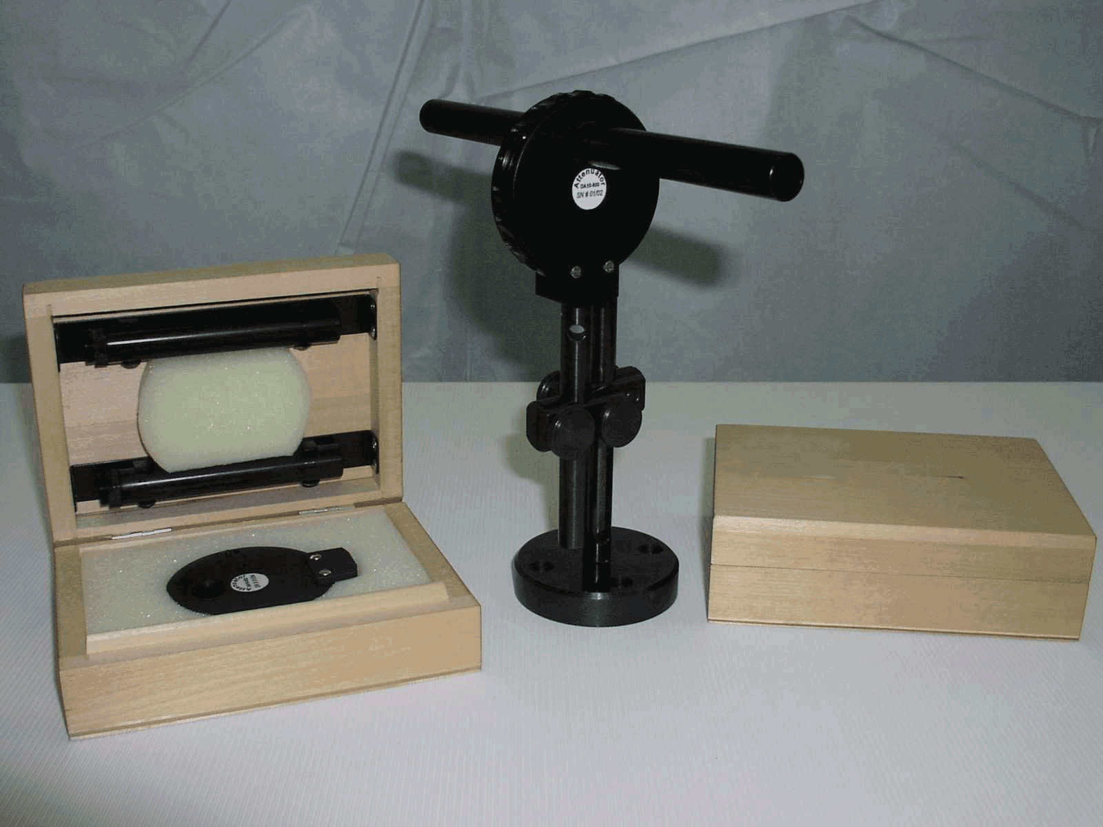
Diffractive Variable Attenuator (DVA) -
buy online
Diffractive Variable Attenuator Housing
-
DVA picture
Femtosecond autocorrelator Reef-RTD 700-1300 nm -
buy online
Hemispherical cylinder
optics
BTO Crystals -
BBO crystals (pdf) -
BBO crystals examples -
800nm>400nm
800nm>266nm -
buy online -
examples
+certificates
LiNbO3 wafers -
buy online -
more details
Stoichiometric LiNbO3 wafers
-
4” Stoichiometric LiNbO3 wafers, YZ-cut
-
stock
Stoichiometric MgO(0.6%):LiNBO3 crystals
Rutile coupling prisms -
brochure -
buy online
-
rutile Brewster
prism -
applications
PPMgOLN 532nm -
PPMgOLN488nm
CaF2
-
CaF2
prism -
CaF2
lenses-
custom -
Ge
-
ZnSe -
dia3.5 -
ZnSe rhomb -
ZnSe
slides -
ZnSe
vacuum viewports -
ZnSe
cylindrical optics -
ZnSe
hemicylindrical prism, 25.4 mm -
Zinc Selenide rhomb -
Germanium
viewport -
BaF2 lens
-
BaF2
meniscus lenses
made of AMTIR-C1 and Germanium substrates with AR/AR coating at 3-5 and 8-12
microns
ZnTe -
CdSe, CdTe, ZnTe wafer inventory
Micro-optics -
Double Concave Lenses
-
Semi-ball lenses -
Ball lenses -
Micro windows -
Micro-prism -
Micro-wedge -
Roof prism -
Rhomboid Prism
Cylindrical and hemispherical lenses
from rutile TiO2
Optics for Infrared Imaging
HEXAGONAL LIGHT PIPE