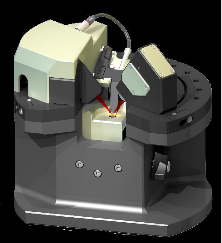
AFM HERON

For the recent years Scanning Probe Microscopy (SPM) has
proved to be the extremely successful technique for characterization of
different nano-sized objects. SPM plays the important role in the outburst of
scientific and commercial activities defined by the term “nanotechnology”. As a
great number of applications for the SPM-based research are becoming more and
more diverse and complex, new challenges and demands arise for the SPM
instrumentation. Unfortunately, still the adjustment of the most modern SPMs
is complicated, time consuming and very much operator-dependant. This drawback
leads to poor reproducibility of the instrument settings and consequently to
poorly reproducible results.
|
New, fully motorized AFM HERON (HERO of Nanotechnology) which allows to perfectly align a cantilever, laser and photodiode by just one click on a command button. The scanning settings and landing parameters are also automated that allows to avoid any time consuming adjustment operations, thus leaving more time to researcher for designing the experiment and performing more accurate measurements. |
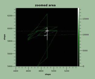 Figure 1. Automated, one-click laser-to-cantilever alignment. |
|
Figure 2. Distribution map of the cantilever's oscillation at the fundamental (left) and second (right) modes. |
Another unique feature of AFM HERON is the
capability to map the distribution of the oscillation amplitude along the
cantilever. After the map is acquired, operator can choose the most
appropriate position of the laser spot on the cantilever for his
measurements. This becomes especially important when a cantilever is excited
at higher modes such as in the Figure 2. The complete automation of the AFM HERON setup allows researchers to avoid time consuming and tiresome routine adjustments and concentrate on the experiment itself, measurements and result interpretation. |
Due to the combination of the low-noise registration
system, unique scanner, advanced electronics and smart scanning procedures
that incorporated over 100 years of combined SPM research experience, with
AFM HERON one can perform unique measurements which are extremely
difficult, if possible at all, using other SPM instruments.
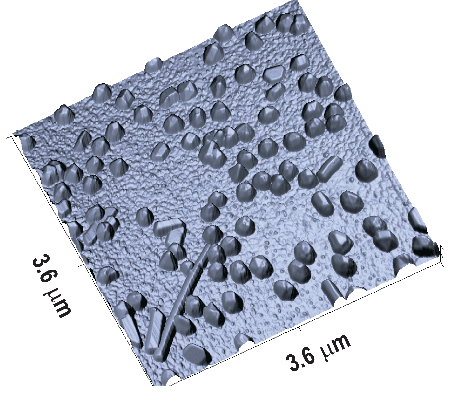 Figure 3. 130 nm Ag nanoparticles immobilized on the metal surface, 3.6x3.6 um scan. |
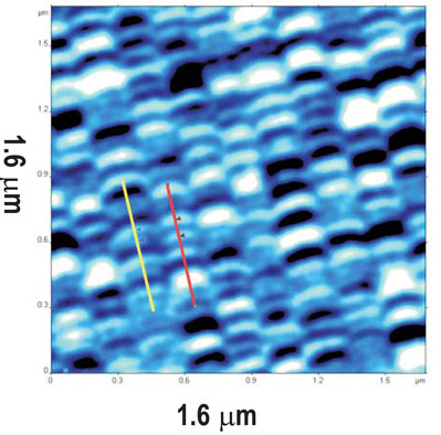
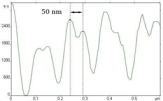
Extra-safe and at the same time fast landing procedure makes it possible to protect even very sharp tips from any possible damage. Due to the availability of the true non-contact scanning mode one can measure even the most fragile and mechanically sensitive samples. Unique smart scanning procedures allow to obtain high quality images on very challenging objects like 130 nm Ag nanoparticles or modern high density hard drive disks.
 |
 |
|
|
|
One of the unique features of HERON AFM is its
scanner. Due to our innovative design and flexure guide technology, this
scanner with built-in capacitive sensors shows the unmatched performance
characteristics (significant scanner natural frequencies come up to 20-30
kHz in XY and up to 35-40 kHz in Z) allowing a significant increase in the
scanning speed without sacrificing the image quality. The scanner allows
high scan rate imaging of samples with coarse topography features. The image
of the 540 nm calibration grating (Fig. 5) is obtained at 10Hz line
frequency.
The advanced digital controller equipped with the optimized scanning control
algorithms allows to decrease the phase lag, overshooting and ringing during
the scanning process, making sure that the quality of the image remains the
same even at higher speeds.
|
Figure 5. Silicon calibration grating. |
The novel proprietary MFM imaging mode allows the user to obtain the magnetic profile of the sample at outstanding speed. This MFM image of the magnetic structure of surface domains in Yttrium Iron Garnet (YIG) film was acquired at 10 Hz scan rate.
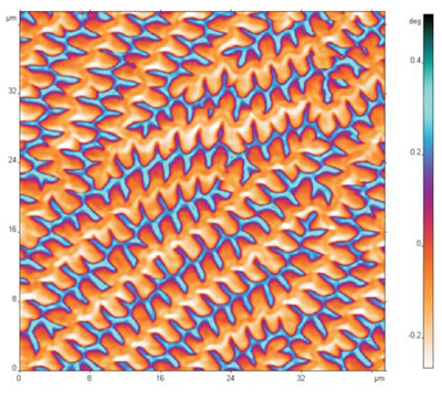 Figure 6. Magnetic structure of surface domains in Yttrium Iron Garnet (YIG) film. |
Due to very well designed and calculated construction of
the AFM and the scanner, HERON AFM features outstanding
mechanical stability, which allows the user to get atomic resolution images
with the same 100 micron scanner and at the same time to produce high
quality images without vibration isolation tables. This is of extreme
importance for the integration of the AFM with the optical facilities on top
of an optical table.
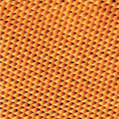 Figure 7. Atomic resolution on HOPG obtained with the 100 micron scanner. AFM contact mode, 32 angstrom scan. |
request additional info and quote
Where Del Mar Photonics product's names come from?
Del Mar means 'by the sea", and Photonics is all about optical waves. So we decided to choose terms popular in surfing and sailing communities. Our femtosecond lasers, amplifiers and systems are named after popular surf breaks around the world, and many other products names after sailing and nautical terms.
HERON AFM is named after after beautiful great blue heron shown below in the surf at Torrey Pines Beach

Del Mar Photonics nano-imaging gallery
High resolution MFM image of Seagate Barracuda 750Gb Hard Drive, ST3750640AS.
130 nm Ag nanoparticles immobilized on the metal surface, 3.6x3.6 um scan
Magnetic structure of surface domains in Yttrium Iron Garnet (YIG) film
Atomic resolution on HOPG obtained with the 100 micron scanner
NSOM Fluorescence image of 100 nm - diameter TransFluoSpheres
Near-field optical image of 250 nm - diameter gold beads, deposited onto a glass
slide
AFM (topography) image of DNA (<3 nm thickness),
deposited onto a glass slide
Near-field optical image of 100 nm - diameter polystyrene beads, deposited onto
a glass slide
Send us your sample for nano-characterization!!!
Related Del Mar Photonics Products:
AFM HERON
Near-field
Scanning Optical Microscope (NSOM)
Femtosecond nanophotonics
Femtosecond NSOM