Del Mar Photonics
New item!
CdSe single crystals with (11-20)
orientation -
request a quote
High-resistivity CdSe single crystals with (11-20) orientation, both
sides polished, unmounted, 10x10x0.5 mm
The following items are available in stock.
Call 1-858-876-3133 for availability or
email us to place your order
while supplies last! Do not see waht you want in the list?
E-mail for a custom quote!
1 CdTe (110), 10 X 8 X 3 mm, 2 sides polished 60/40, high resistivity (>/= 10^6
Ohm*cm), n-type, 1 pc.
2 CdTe, 5 X 5 X 1.3 mm, (110) at 45deg to 5 X 5 mm, 2 sides polished 60/40, high
resistivity (>/= 10^6 Ohm*cm), 7 pcs.
3 CdTe, 6 X 4 X 2 mm, 6 X 4 // (111), all sides polished 60/40, high resistivity
(>/= 10^6 Ohm*cm), 8 pcs.
4 CdTe, Dia: 6 X 8 mm, Dia: 6 //(111), high resistivity (>/= 10^6 Ohm*cm), 2
pcs.
5 CdTe, Dia: 15 X 2 mm, (110), 2 sides polished 60/40, high resistivity (>/=
10^6 Ohm*cm), 3 pcs.
6 CdTe, 10 X 10 X 1 mm, random oriented, 2 sides inspection polished, high
resistivity (>/= 10^6 Ohm*cm), 4 pcs.
7 CdTe, 7 X 5 X 0.5 mm, (110), 3 sides polished 60/40, high resistivity(>/= 10^6
Ohm*cm), 5 pcs.
8 CdTe, 30 X 2 X 1 mm, 30 X 2 // (110), 2 sides polished 60/40, high resistivity
(>/= 10^6 Ohm*cm), 3 pcs.
9 CdTe, Dia: 27 X 1.5 mm, (111), 2 sides polished 60/40, high resistivity (>/=
10^6 Ohm*cm),1 pc.
10 CdTe, 30 X 3 X 3 mm, 30 X 3 // (111), 3 X 3 // (110), all sp 60/40, high
resistivity (>/= 10^6 Ohm*cm), 2 pcs.
11 CdTe, 10 X 10 X 0.5 mm, (110), 1 side polished 60/40, 1 side fine grinded,
low resistivity, p-type, 2 pcs.
12 CdTe, 10 X 10 X 0.2 mm, (110), 2 sides polished 60/40, high resistivity (>/=
10^6 Ohm*cm), 1 pc.
13 CdTe, 10 X 5 X 1 mm, (110), 2 sides polished 60/40, high resistivity(>/= 10^6
Ohm*cm), 1 pc.
14 CdTe, 5 X 5 X 2 mm, (110), 2 sides polished 60/40, high resistivity (>/= 10^6
Ohm*cm), 1 pc.
15 CdTe, 10 X 10 X 2 mm, (110)/(110)/(100), 2 sides polished 60/40, high
resistivity (>/= 10^6 Ohm*cm), 1 pcs.
16 CdTe, 10 X 10 X 0.5 mm, (100), 1 side polished 60/40, 1 side fine grinded,
p-type, 3 pcs.
17 CdTe, 10 X 10 X 0.5 mm, random oriented, 1 side polished 60/40, 1 side fine
grinded, p-type, 7 pcs.
18 CdTe, 10 X 10 X 0.5 mm, (100), 2 sides polished 60/40, p-type, 2 pcs.
19 CdTe, 10 X 10 X 0.5 mm, (110), 2 sides polished 60/40, high resistivity (>/=
10^6 Ohm*cm), 1 pc.
20 CdTe, 10 X 10 X 0.5 mm, (111), 2 sides polished 60/40, high resistivity (>/=
10^6 Ohm*cm), 1 pc.
21 CdTe, 10 X 10 X 1 mm, (100), 2 sides polished 60/40, high resistivity (>/=
10^6 Ohm*cm), 4 pcs.
22 CdTe, 20 X 20 X 1 mm, (110), 2 sides polished 40/20, high resistivity (>/=
10^6 Ohm*cm), 1 pc.
1 ZnTe 10 x 10 x 0.5 mm, (110), 2 sides polished 60/40, 3pcs.
2 ZnTe 10 x 8 x 0.8 mm, (110), 2 sides polished 60/40, 2pcs.
3 ZnTe 10 x 8 x 0.2 mm, (110), 2 sides polished 60/40, 1pc.
4. ZnTe 10 x 8 x 1 mm, (110), 2 sides polished 60/40, 2pcs.
5. ZnTe 10 x 10 x 0.4 mm, (110), 2 sides polished 60/40, 1pc.
1 CdSe powder 10-30 um (within 1 batch), 99.999 %, 10 kg.
2 CdSe, 6 X 4 X 2 mm, 6 X 4 // (0001), all sides polished 60/40, high
resistivity (>/= 10^11 Ohm*cm), 11 pcs.
3 CdSe, random oriented, 10 X 10 X 0.5mm, 2 sides polished 60/40, high
resistivity (>/= 10^11 Ohm*cm), 1 pc.
4 CdSe (10-10), 25X15X1 mm, 2 sides polished 60/40, low resistivity (< 1
Ohm*cm), 2 pc.
5 CdSe, Dia: 12.7 X 3.2 mm, <0001> // Dia: 12.7, 2 sides polished 60/40, high
resistivity (>/= 10^11 Ohm*cm), 1 pc.
6 CdSe, Dia: 10 X 0.3 mm, // "c", polished 60/40, 5 pcs.
7 CdSe, 5X5X0.5 mm, (0001), all sides polished 60/40, high resistivity (>/=
10^11 Ohm*cm), 5 pcs.
8 CdSe, (0001), 10 X 10 X 0.5 mm, 1 side polished 60/40, 1 side grinded, low
resistivity (< 1 Ohm*cm), 7 pcs.
9 CdSe, // "c", 10 X 10 X 1 mm, 2 sides polished 60/40, low resistivity (< 1
Ohm*cm), 5 pcs.
10 CdSe Dia: 5 X 5 mm, (0001), 2 sides polished 60/40. High resistivity (>/=
10^11 Ohm*cm), 4 pcs.
11 CdSe, 5 X 5 X 1 mm, (0001), all sides polished 60/40, low resistivity(< 1
Ohm*cm), 10 pcs.
12 CdSe, random oriented, 10 X 10 X 0.5 mm, 2 sides polished 60/40, low
resistivity (< 1 Ohm*cm), 9 pcs.
Call 1-858-876-3133 for availability or
email us to place your order
while supplies last! Do not see waht you want in the list?
E-mail for a custom quote!
Del Mar Photonics
Cadmium telluride (CdTe) is a crystalline compound formed from cadmium and
tellurium. It is used as an infrared optical window and a solar cell material.
It is usually sandwiched with cadmium sulfide to form a p-n junction
photovoltaic solar cell. Typically, CdTe cells use a n-i-p structure.
Applications
CdTe is a highly useful material in the making of thin film solar cells.
Thin-film CdTe provides a cost-effective solar cell design, but is less
efficient than polysilicon.
CdTe can be alloyed with mercury to make a versatile infrared detector material
(HgCdTe). CdTe alloyed with a small amount of zinc makes an excellent
solid-state X-ray and gamma ray detector (CdZnTe).
CdTe is used as an infrared optical material for optical windows and lenses but
it has small application and is limited by its toxicity such that few optical
houses will consider working with it. An early form of CdTe for IR use was
marketed under the trademarked name of Irtran-6 but this is obsolete.
CdTe is also applied for electro-optic modulators. It has the greatest
electro-optic coefficient of the linear electro-optic effect among II-VI
compound crystals (r41=r52=r63=6.8×10⁻¹² m/V).
CdTe doped with chlorine is used as a radiation detector for x-rays, gamma rays,
beta particles and alpha particles. CdTe can operate at room temperature
allowing the construction of compact detectors for a wide variety of
applications in nuclear spectroscopy.[1] The properties that make CdTe superior
for the realization of high performance gamma- and x-ray detectors are high
atomic number, large bandgap and high electron mobility ~1100 cm2/V·s, which
result in high intrinsic μτ (mobility-lifetime) product and therefore high
degree of charge collection and excellent spectral resolution.
Physical properties
Lattice constant: 0.648 nm at 300K
Young's modulus: 52 GPa
Poisson ratio: 0.41
Thermal properties
Thermal conductivity: 6.2 W·m/m2·K at 293 K
Specific heat capacity: 210 J/kg·K at 293 K
Thermal expansion coefficient: 5.9×10⁻⁶/K at 293 K[2]
Optical and electronic properties
Fluorescence spectra of colloidal CdTe quantum dots of various sizes, increasing
approximately from 2 to 20 nm from left to right. The red shift of fluorescence
is due to quantum confinement.
Bulk CdTe is transparent in the infrared, from close to its band gap energy
(1.44 eV at 300 K,[3] which corresponds to infrared wavelength of about 860 nm)
out to wavelengths greater than 20 µm; correspondingly, CdTe is fluorescent at
790 nm. When the size of CdTe crystal is being reduced to a few nanometers and
below, thus making a CdTe quantum dot, the fluorescence peak shifts towards
through the visible range to the ultraviolet.
Chemical properties
CdTe has very low solubility in water. It is etched by many acids including
hydrochloric, and hydrobromic acid, forming (toxic) hydrogen telluride gas and
toxic cadmium salts. It is a reducing agent and is unstable in air at high
temperatures.
Cadmium telluride is commercially available as a powder, or as crystals. It can
be made into nanocrystals.
Toxicity
Cadmium telluride is toxic if ingested, if its dust is inhaled, or if it is
handled improperly (i.e. without appropriate gloves and other safety
precautions). Once properly and securely captured and encapsulated, CdTe used in
manufacturing processes may be rendered harmless. CdTe appears to be less toxic
than elemental cadmium, at least in terms of acute exposure.[4]
The toxicity is not solely due to the cadmium content. One study found that the
highly reactive surface of cadmium telluride quantum dots triggers extensive
reactive oxygen damage to the cell membrane, mitochondria, and cell nucleus.[5].
In addition, the cadmium telluride films are typically recrystallized in a toxic
solution of cadmium chloride.
The disposal and long term safety of cadmium telluride is a known issue in the
large scale commercialization of cadmium telluride solar panels. Serious efforts
have been made to understand and overcome these issues. A document hosted by the
U.S. National Institutes of Health[6] dated 2003 discloses that:
Brookhaven National Laboratory (BNL) and the U.S. Department of Energy (DOE) are
nominating Cadmium Telluride (CdTe) for inclusion in the National Toxicology
Program (NTP). This nomination is strongly supported by the National Renewable
Energy Laboratory (NREL) and First Solar Inc. The material has the potential for
widespread applications in photovoltaic energy generation that will involve
extensive human interfaces. Hence, we consider that a definitive toxicological
study of the effects of long-term exposure to CdTe is a necessity.
Researchers from the U.S. Department of Energy's Brookhaven National Laboratory
have found that large-scale use of CdTe PV modules does not present any risks to
health and the environment, and recycling the modules at the end of their useful
life completely resolves any environmental concerns. During their operation,
these modules do not produce any pollutants, and furthermore, by displacing
fossil fuels, they offer great environmental benefits. CdTe PV modules appear to
be more environmentally friendly than all other current uses of Cd.[7]
The approach to CdTe safety in the European Union and China is much more
cautious: cadmium and cadmium compounds are considered as toxic carcinogens in
EU whereas China regulations allow Cd products for export only.[8][9]
References
P. Capper (1994). Properties of Narrow-Gap Cadmium-Based Compounds. London, UK:
INSPEC, IEE. ISBN 0-85296-880-9.
Palmer, D W (March 2008). "Properties of II-VI Compound Semiconductors".
Semiconductors-Information.
Bube, R. H. (1955). "Temperature dependence of the width of the band gap in
several photoconductors". Physical Review 98: 431–3.
(PDF) Acute Oral and Inhalation Toxicities in Rats With Cadmium Telluride.
International Journal of Toxicology. 2009-08.
"Unmodified Cadmium Telluride Quantum Dots Prove Toxic". Nano News (National
Cancer Institute). 2005-12-12.
(PDF) Nomination of Cadmium Telluride to the National Toxicology Program. United
States Department of Health and Human Services. 2003-04-11.
Fthenakis, V M (2004). "Life Cycle Impact Analysis of Cadmium in CdTe PV
Production". Renewable & Sustainable Energy Reviews 8: 303–334.
doi:10.1016/j.rser.2003.12.001.
Sinha, Parikhit; Kriegner, Christopher J.; Schew, William A.; Kaczmar,
Swiatoslav W.; Traister, Matthew; Wilson, David J. (2008). "Regulatory policy
governing cadmium-telluride photovoltaics: A case study contrasting life cycle
management with the precautionary principle". Energy Policy 36: 381.
doi:10.1016/j.enpol.2007.09.017.
Cadmium Telluride Casts Shadow of Death on First Solar
Del Mar Photonics -
Newsletter December 2010 -
Newsletter
April 2011
Product news and updates - Training Workshops
- Featured Customer - Other News
 |
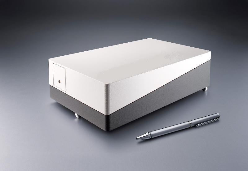
Trestles LH Ti:Sapphire
laser
Trestles LH is a new series of high quality femtosecond Ti:Sapphire
lasers for applications in scientific research, biological imaging, life
sciences and precision material processing. Trestles LH includes integrated
sealed, turn-key, cost-effective, diode-pumped
solid-state (DPSS). Trestles LH lasers offer the most attractive pricing
on the market combined with excellent performance and reliability. DPSS LH
is a state-of-the-art laser designed for today’s applications. It combines
superb performance and tremendous value for today’s market and has
numerous advantages over all other DPSS lasers suitable for Ti:Sapphire
pumping. Trestles LH can be customized to fit customer requirements and
budget. Reserve a
spot in our Femtosecond lasers training
workshop in San Diego, California. Come to learn how to build a
femtosecond laser from a kit
|
 |
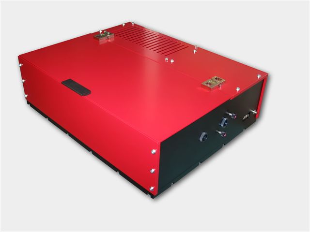
DPSS DMPLH lasers
DPSS DMP LH series lasers will pump your Ti:Sapphire laser.
There are LH series lasers installed all over the world pumping all makes & models
of oscillator. Anywhere from CEP-stabilized femtosecond Ti:Sapphire oscillators
to ultra-narrow-linewidth CW Ti:Sapphire oscillators. With up to 10 Watts CW
average power at 532nm in a TEMoo spatial mode, LH series
lasers has quickly proven itself
as the perfect DPSS pump laser for all types of Ti:Sapphire or dye laser.
Ideal for pumping of:
Trestles LH
Ti:Sapphire laser
T&D-scan laser
spectrometer based on narrow line CW Ti:Sapphire laser
|
 |
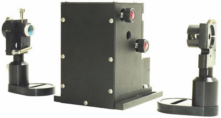
Pismo pulse picker
The Pismo pulse picker systems is as a pulse gating system that lets single
pulses or group of subsequent pulses from a femtosecond or picosecond pulse
train pass through the system, and stops other radiation. The system is
perfectly suitable for most commercial femtosecond oscillators and
amplifiers.
The system can pick either single pulses, shoot bursts (patterns of single
pulses) or pick group of subsequent pulses (wider square-shaped HV pulse
modification). HV pulse duration (i.e. gate open time) is 10 ns in the default
Pismo 8/1 model, but can be customized from 3 to 1250 ns upon request or made
variable. The frequency of the picked pulses starts with single shot to 1 kHz
for the basic model, and goes up to 100 kHz for the most advanced one.
The Pockels cell is supplied with a control unit that is capable of synching
to the optical pulse train via a built-in photodetector unit, while electric
trigger signal is also accepted. Two additional delay channels are available
for synching of other equipment to the pulse picker operation. Moreover, USB
connectivity and LabView-compatible drivers save a great deal of your time
on storing and recalling presets, and setting up some automated experimental
setups. One control unit is capable of driving of up to 3 Pockels cells, and
this comes handy in complex setups or contrast-improving schemes. The system
can also be modified to supply two HV pulses to one Pockels cell unit,
making it a 2-channel pulse picker system. This may be essential for
injection/ejection purposes when building a regenerative or multipass
amplifier system.
|
 |
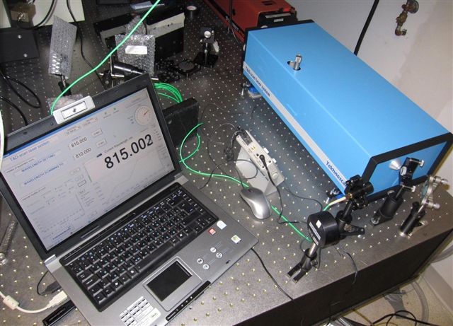
New laser spectrometer
T&D-scan for research that
demands high resolution and high spectral
density in UV-VIS-NIR spectral domains - now available with
new pump option!
The
T&D-scan
includes
a CW ultra-wide-tunable narrow-line laser, high-precision wavelength meter,
an electronic control unit driven through USB interface as well as a
software package. Novel advanced design of the fundamental laser component
implements efficient intra-cavity frequency doubling as well as provides a
state-of-the-art combined ultra-wide-tunable Ti:Sapphire & Dye laser
capable of covering together a
super-broad spectral range between 275 and 1100 nm. Wavelength
selection components as well as the position of the non-linear crystal are
precisely tuned by a closed-loop control
system, which incorporates highly accurate wavelength meter.Reserve a
spot in our CW lasers training
workshop in San Diego, California. Come to
learn how to build a
CW
Ti:Sapphire laser from a kit
|
 |
Near IR viewers
High performance infrared
monocular viewers are designed to observe radiation emitted by
infrared sources. They can be used to observe indirect radiation of IR
LED's and diode lasers, Nd:YAG, Ti:Sapphire, Cr:Forsterite, dye lasers and
other laser sources. IR viewers are ideal for applications involving the
alignment of infrared laser beams and of optical components in
near-infrared systems. Near IR viewers
sensitive to laser radiation up to 2000 nm.
The light weight, compact monocular may be used as a hand-held or facemask
mounted for hands free operation.
Ultraviolet viewers are
designed to observe radiation emitted by UV sources. |
 |
AOTF Infrared Spectrometer
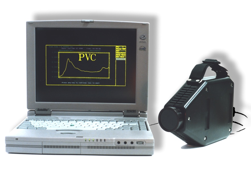
Del Mar Photonics offer a handheld
infrared spectrometer based on the
acousto-optic tunable filter (AOTF). This instrument is about the size and
weight of a video camera, and can be battery operated. This unique, patented
device is all solid-state with no moving parts. It has been sold for a wide
variety of applications such as liquid fuel analysis, pharmaceutical analysis,
gas monitoring and
plastic analysis.
Miniature AOTF infrared spectrometer uses
a crystal of tellurium dioxide to scan the wavelength. Light from a light source enters
the crystal, and is diffracted into specific wavelengths. These wavelengths are
determined by the frequency of the electrical input to the crystal. Since there
are no moving parts, the wavelength scanning can be extremely fast. In addition,
specific wavelengths can be chosen by software according to the required algorithm, and therefore can be modified without changing the
hardware. After the infrared radiation reflects off of the sample, it is
converted into an electrical signal by the detector and analyzed by the
computer. Del Mar Photonics is looking for international distributors for
RAVEN - AOTF IR spectrometer for plastic identification and for variety of
scientific and industrial collaborations to explore futher commercial potential
of AOTF technology.
New:
AOTF spectrometer to measure lactose, fat and proteins in milk
|
 |
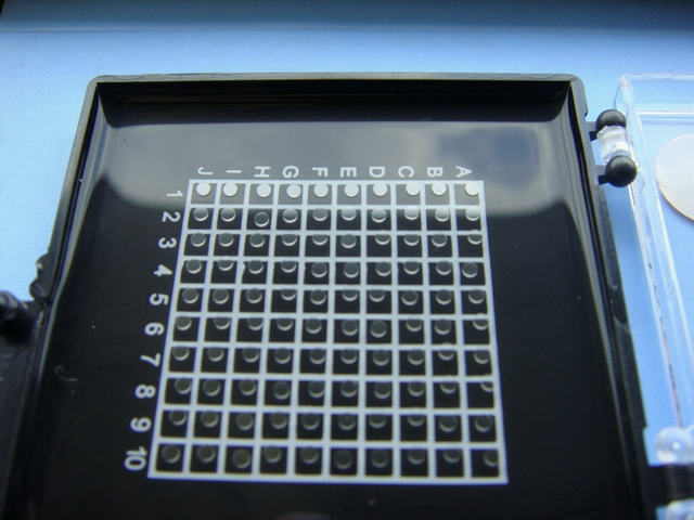
Open Microchannel Plate Detector
MCP-MA25/2 -
now in stock!
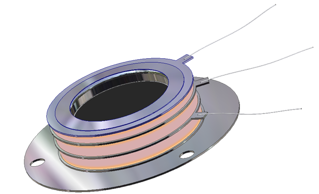
Microchannel Plate Detectors MCP-MA series are an open MCP detectors
with one or more microchannel plates and a single metal anode. They are intended
for time-resolved detection and make use of high-speed response properties of
the MCPs. MCP-MA detectors are designed for photons and particles detection in
vacuum chambers or in the space.
MCP-MA detectors are used in a variety of applications including UV, VUV and EUV
spectroscopy, atomic and molecular physics, TOF mass–spectrometry of clusters
and biomolecules, surface studies and space research.
MCP-MA detectors supplied as a totally assembled unit that can be easily mounted
on any support substrate or directly on a vacuum flange. They also can be
supplied premounted on a standard ConFlat flanges.
buy online -
ask for research discount!
|
 |
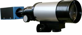
Hummingbird EMCCD camera
The digital Hummingbird
EMCCD camera combines high sensitivity, speed and high resolution.
It uses Texas Instruments' 1MegaPixel Frame Transfer Impactron device which
provides QE up to 65%.
Hummingbird comes with a standard CameraLink output.
It is the smallest and most rugged 1MP EMCCD camera in the world.
It is ideally suited for any low imaging application such as hyperspectral
imaging, X-ray imaging, Astronomy and low light surveillance.
It is small, lightweight, low power and is therefore the ideal camera for
OEM and integrators.
buy online |
 |
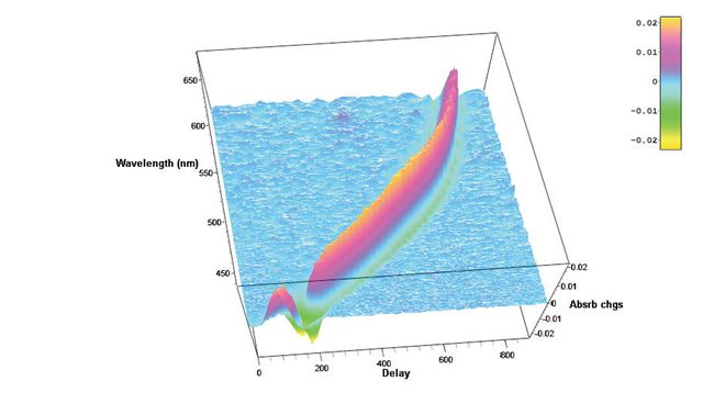
Hatteras-D
femtosecond transient absorption data acquisition system
Future nanostructures and biological nanosystems will take
advantage not only of the small dimensions of the objects but of the
specific way of interaction between nano-objects. The interactions
of building blocks within these nanosystems will be studied and optimized on
the
femtosecond time scale - says Sergey Egorov, President and CEO of Del Mar
Photonics, Inc. Thus we put a lot of our efforts and resources into the
development of new Ultrafast
Dynamics Tools such as our Femtosecond Transient Absorption Measurements
system Hatteras. Whether you want to
create a new photovoltaic system that will efficiently convert photon energy
in charge separation, or build a molecular complex that will dump photon energy
into local heat to kill cancer cells, or create a new fluorescent probe for
FRET microscopy, understanding of internal dynamics on femtosecond time scale
is utterly important and requires advanced measurement techniques.Reserve a
spot in our Ultrafast Dynamics Tools
training workshop in San Diego, California.
|
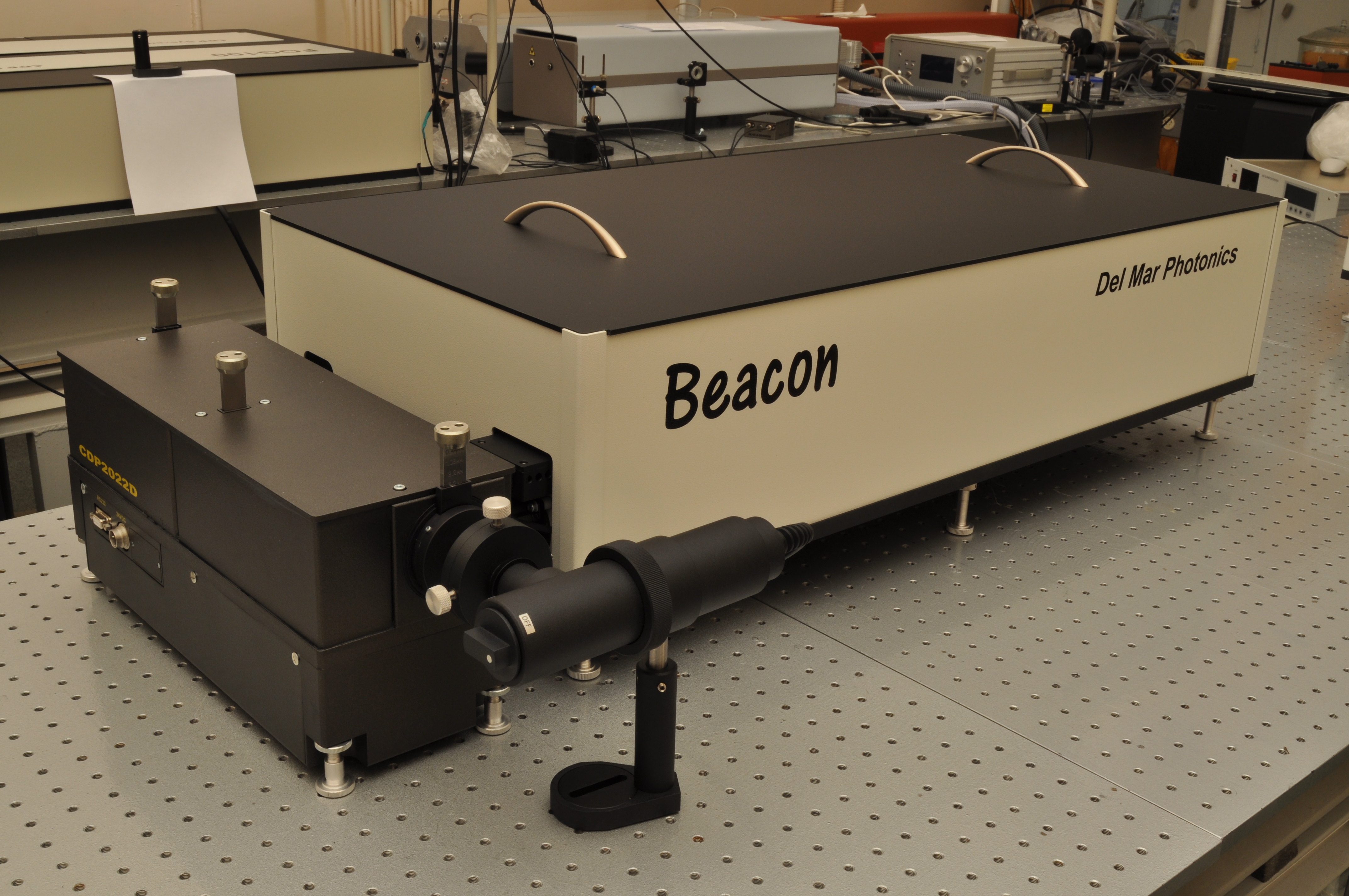 |
Beacon Femtosecond Optically Gated Fluorescence Kinetic Measurement System
-
request a quote -
pdf
Beacon together with Trestles Ti:sapphire oscillator, second and third harmonic
generators. Femtosecond optical gating (FOG) method gives best temporal
resolution in light-induced fluorescence lifetime measurements. The resolution
is determined by a temporal width of femtosecond optical gate pulse and doesn't
depend on the detector response function. Sum frequency generation (also called
upconversion) in nonlinear optical crystal is used as a gating method in the
Beacon femtosecond fluorescence kinetic measurement system. We offer
Beacon-DX for operation together with Ti: sapphire femtosecond oscillators
and Beacon-DA for operation together with femtosecond amplified pulses.
Reserve a
spot in our Ultrafast Dynamics Tools
training workshop in San Diego, California.
|
 |
Wavefront Sensors: ShaH Family
A family of ShaH wavefront sensors represents recent progress of Del Mar
Photonics in Shack-Hartmann-based technology. The performance of Shack-Hartmann
sensors greatly depends on the quality of the lenslet arrays used. Del Mar
Photonics. developed a proprietary process of lenslet manufacturing, ensuring
excellent quality of refractive lenslet arrays. The arrays can be AR coated on
both sides without interfering with the micro-lens surface accuracy. Another
advantage of the ShaH wavefront sensors is a highly optimized processing code.
This makes possible real-time processing of the sensor data at the rate
exceeding 1000 frames per second with a common PC. Due to utilizing low-level
programming of the video GPU, it is possible to output the wavefront data with a
resolution up to 512x512 pixels at a 500+ Hz frame rate. This mode is favorable
for controlling modern LCOS wavefront correctors.
The family of ShaH wavefront sensors includes several prototype models, starting
from low-cost ShaH-0620 suitable for teaching laboratory to a high-end
high-speed model, ShaH-03500. The latter utilizes a back-illuminated EM-gain CCD
sensor with cooling down to -100°C. This makes it possible to apply such a
wavefront sensor in astronomy, remote sensing, etc.
|
 |
Terahertz systems, set ups and components
New band pass and long pass THz optical filters based on porous silicon and metal mesh technologies.
Band pass filters with center wavelengths from 30 THz into GHz range and transmissions up to 80% or better. Standard designs
with clear aperture diameters from 12.5 to 37.5 mm.
Long pass filters with standard rejection edge wavelengths from 60 THz into GHz range. Maximum transmission up to 80% or
better, standard designs at 19.0 and 25.4 mm diameters.
Excellent thermal (from cryogenic to 600 K) and mechanical properties
THz products:
THz Spectrometer kit with Antenna
THz transmission setup
THz time domain spectrometer Pacifica fs1060pca
THz time domain spectrometer Pacifica fs780pca
THz detectors: Golay cell and LiTaO3 piroelectric detectors
PCA - Photoconductive Antenna as THz photomixer
Pacifica THz Time Domain Spectrometer - Trestles Pacifica
Holographic Fourier Transform Spectrometer for THz Region
Wedge TiSapphire Multipass Amplifier System - THz pulses generation
Terahertz Spectroscopic Radar Mobile System for Detection of Concealed Explosives
Band pass filters with center wavelengths from 30 THz into GHz range
Long pass filters with standard rejection edge wavelengths from 60 THz into GHz range
Generation of THz radiation using lithium niobate
Terahertz crystals (THz): ZnTe, GaAs, GaP, LiNbO3 - Wedge ZnTe
|
 |
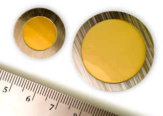
iPCA - interdigital Photoconductive Antenna for terahertz waves
Large area broadband antenna with lens array and high emitter conversion
efficiency
iPCA with LT-GaAs absorber, microlens array for laser excitation wavelengths
l £ 850
nm, adjusted hyperhemispherical silicon lens with a high power conversion
efficiency of 0.2 mW THz power / W optical power. The iPCA can be used also
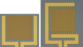
as large area THz detector. The two types iPCAp and iPCAs have the same
active interdigital antenna area but different contact pad directions with
respect to the electrical THz field.
Interdigital Photoconductive Antenna for terahertz waves generation using
femtosecond Ti:Sapphire laser
THz books |
|
|
Fifth Harmonic Generator for
Nd:YAG lasers
The Fifth Harmonic Generator model LG105 is compatible with any pulsed
Nd:YAG laser, and is designed to produce UV-radiation at 213 nm. The
Nd:YAG laser, equipped with LG105, is a versatile device, and in many
applications can eliminate the necessity for excimer lasers. Solid state
technology that does not use toxic gases and costs less gives you the
advantages of both consistent, day-to-day operation and low maintenance. A
high quality BBO crystal is used in the LG105 as the non-linear element,
providing up to 20% conversion efficiency into 213 nm. The non-linear
crystal is placed in a special cell ensuring long lifetime of BBO without
any degradation or breakage. A harmonic separation system installed in LG105
provides nearly 100 % spectral purity of the output at 213 nm. The LG105
Fifth Harmonic Generator gives you not only high power output but also
excellent radiation stability
|
 |
IntraStage lowers the cost
of test data management!
Struggling with gigabytes or terabytes of test data?
IntraStage easily transforms test
data from disparate sources into web-based quality metrics and engineering
intelligence you can use.
Contact
us today to discuss your test management requirements and specifications of your
application.
|
Training Workshops
Featured Customer
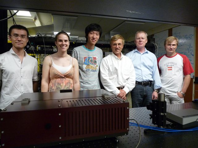 |
Trestles LH10-fs/CW laser system at UC Santa Cruz Center of
Nanoscale Optofluidics
Del
Mar Photonics offers new
Trestles fs/CW laser system which can be easily
switched from femtosecond mode to CW and back. Having both modes of operation in one system dramatically increase a
number of applications that the laser can be used for, and makes it an ideal
tool for scientific lab involved in multiple research projects.
Kaelyn Leake is a PhD student in Electrical Engineering. She graduated from
Sweet Briar College with a B.S. in Engineering Sciences and Physics. Her
research interests include development of nanoscale optofluidic devices and
their applications. Kaelyn is the recipient of a first-year QB3 Fellowship.
In this video Kaelyn talks about her experimental research in nanoscale
optofluidics to be done with Trestles LH laser.
Reserve a spot in our
femtosecond Ti:Sapphire training workshop in San
Diego, California during summer 2011 |
 |
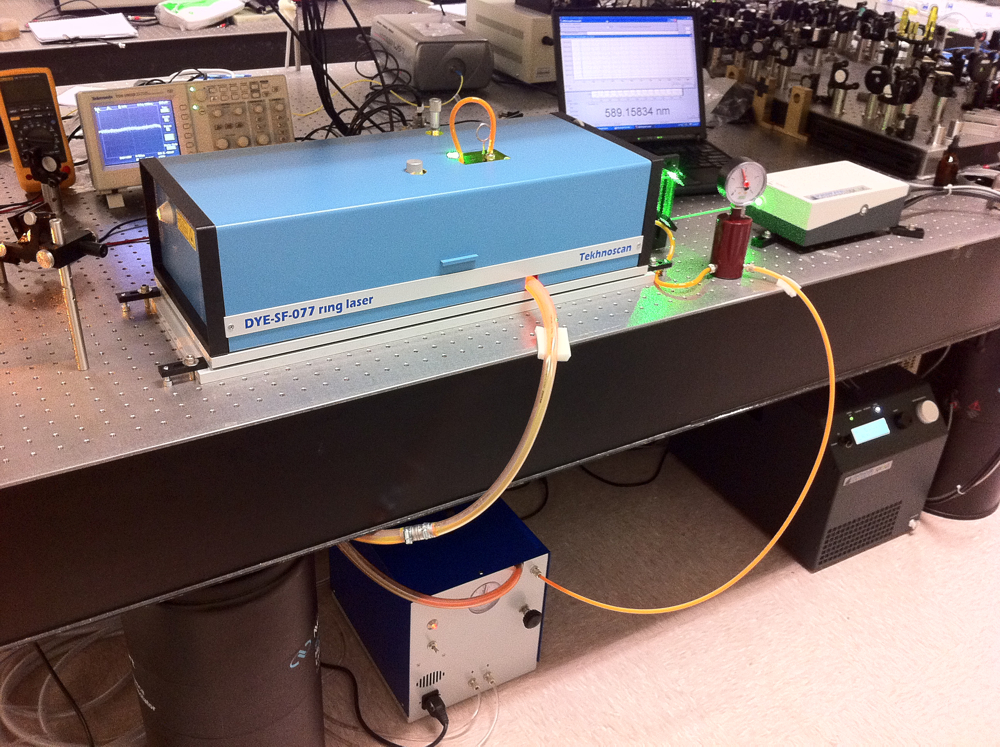
Frequency-stabilized CW
single-frequency ring Dye laser DYE-SF-007 pumped by DPSS DMPLH laser installed
in the brand new group of Dr. Dajun Wang at the The Chinese University of Hong
Kong.
DYE-SF-077 features exceptionally narrow generation line width, which
amounts to less than 100 kHz. DYE-SF-077 sets new standard for generation
line width of commercial lasers. Prior to this model, the narrowest line-width
of commercial dye lasers was as broad as 500 kHz - 1 MHz. It is necessary to
note that the 100-kHz line-width is achieved in DYE-SF-077 without the use of an
acousto-optical modulator, which, as a rule, complicates the design and
introduces additional losses. A specially designed ultra-fast PZT is used for
efficient suppression of radiation frequency fluctuations in a broad frequency
range. DYE-SF-077 will be used in resaerch of Ultracold polar molecules,
Bose-Einstein condensate and quantum degenerate Fermi gas and High resolution
spectroscopy |
Other News
Optical Society of Southern California meeting at UCSD OSSC 2011-04-27
Nd:YAG laser ordered by the University of Leon, UANL, Mexico
Wedge 50 Multipass Amplifier pumped with a Darwin-527-30-M DPSS Laser
ordered by Hong Kong customer
New
Trestles LH10-fs/CW femtosecond+CW laser ready for delivery to the
University of California Santa Cruz
Trestles femtosecond
Ti:Sapphire laser delivered to North Carolina State
University
Del Mar Photonics sponsor IONS (International OSA Network of Students)
conference IONS-NA-2 in Tucson, Arizona
IONS-NA-2
website
Best talk and best
poster awards at IONS-Moscow 2010 conference sponsored by Del Mar Photonics
Watch Del Mar Photonics
videos!
Del Mar Photonics is now on Twitter!
Del Mar Photonics featured components
Del Mar Photonics continuously expands its components
portfolio.

|
Solar
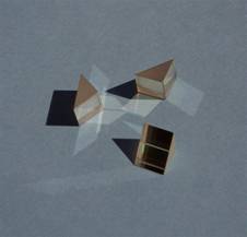
Prisms for Concentrating Photovoltaic Systems (CPV)
Solar cells made of compound semiconductors such
as gallium arsenide are very expensive. Usually very small cells are
installed and various means such as mirrors, lenses, prisms, etc..are used
to concentrate sunlight on the cells. Concentration photovoltaic technology
(CPV) uses the solar radiation with an efficiency of 40%, double that of
conventional solar cells
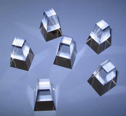
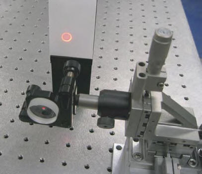
Del Mar Photonics design custom Concentrating Photovoltaic Systems (CPV) and
supply variety of the optical components for CPV such as
solar prisms shown in the picture.
hexagonal light pipes,
optical rods |
|
Axicon Lens
Axicon lens also known as conical lens or rotationally symmetric prism is
widely used in different scientific research and application. Axicon can be
used to convert a parallel laser beam into a ring, to create a non
diffractive Bessel beam or to focus a parallel beam into long focus depth.
Del Mar Photonics supplies axicons with cone angles range from 130° to
179.5° for use with virtually any laser radiation. We manufacture and supply
axicons made from BK7 glass, fused silica and other materials.
download brochure -
request a quote |
 |
Rutile (TiO2) coupling
prisms
Del Mar Photonics offers optical elements made of high quality synthetically
grown Rutile Titanium Dioxide crystals. Rutile’s strong birefringency, wide
transmission range and good mechanical properties make it suitable for
fabrication of polarizing cubes, prisms and optical isolators. Boules having
high optical transmission and homogeneity are grown by proprietary method.
Typical boules have 10 - 15 mm in dia. and up to 25 mm length. Optical
elements sizes - from 2 x 2 x 1 mm to 12.7 x 12.7 x 12.7 mm. Laser grade
polish quality is available for finished elements. So far we the largest
elements that we manufactured are 12 x15 x 5 mm, in which optical axis is
parallel to 15 mm edge, 5 mm is along beam path, 12 x 15 mm faces polished
20/10 S/D, one wave flatness, parallelism < 3 arc.min. (better specs.
available on request).
more details -
download brochure -
request a quote |
 |
Sapphire components
Sapphire
Circular Windows -
Square & Rectangle - Rods
Sapphire & Ruby
Rings - Sapphire
& Ruby Balls -
Sapphire & Ruby Nozzles
Sapphire Lenses -
Ball & Seat -
Special Products
- Sapphire Vee
& Cup Jewels
Sapphire Ceramics -
Ceramic Sleeves
- Ceramic Holes -
Ceramic Rods
Sapphire & Ruby
Orifices -
Sapphire & Ruby Tubes -
Sapphire Components
Sapphire Half
Round Rod - Sapphire
Windows -
Rods &
Tubes - Special
Part
Sapphire Prism -
Sapphire Chisel -
Sapphire
Square Rod |
 |
Vacuum viewport
Del Mar Photonics offer a range of competitively priced UHV viewports ,
Conflat, ISO or KF including a variety of coatings to enhance performance.
Del Mar Photonics viewports are manufactured using advanced techniques for
control of special and critical processes, including 100 percent helium leak
testing and x-ray measurements for metallization control. Windows Materials
include: Fused silica, Quartz , Sapphire , MgF2, BaF2, CaF2, ZnSe, ZnS, Ge,
Si, Pyrex. Standard Viewing diameters from .55" to 1.94 ".
Coating - a range of custom coatings can applied - which include
- Single QWOT
- Broad Band AR
- V coatings
- ITO
- DLC (Diamond like coating)
more
details -
request a
quote
|
 |
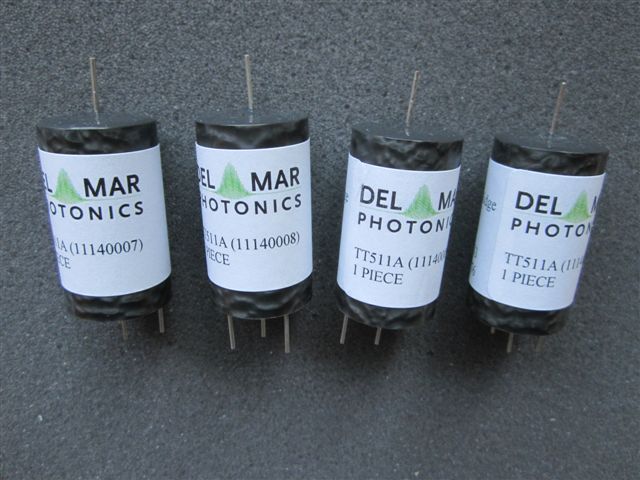
Hydrogen
Thyratrons are used in
such devices as radars with different power levels, high-power pulsed
technical, electrophysical, medical devices and lasers. Sophisticated
design and high quality ceramic-metal envelope determines long lifetime
and very accurate and reliable operation of hydrogen thyratrons under wide range of environmental
conditions.
Applications:
- radars
- pulsed lasers power supplies
- medical apparatus
- electrophysical instrumentation
Triggered Three-Electrode Spark Gap Switches are ceramic-metal sealed off gas
discharge trigatron-type devices with a co-axial trigger electrode. These Gas
Discharge Tubes contain no mercury and, due to an advanced design, feature high
reliability and a long lifetime being operating under wide range of
environmental conditions.
Applications:
- pulsed installation for processing materials
- installations with plasma focus
- pulse power supplies for lasers and other pulse equipment
- medical apparatus such as lithotriptors and defibrillators
- processing systems for petroleum wells |

|
Trigger Transformers
Del Mar Photonics supply
trigger transformers for triggered spark gaps and
other applications.
Contact us to today to discuss your application or requesta quote.
Trigger Transformers are used to provide a fast high voltage pulse up to
30kV/µs and more. This high voltage pulse is applied to the trigger
electrode to initiate switching action in the
three-electrode
spark gaps. Either positive or negative pulses can be obtained from all
of the transformers. |
 |
We are looking forward to hear from you and help you with
your optical and crystal components requirements. Need time to think about
it?
Drop us a line and we'll send you beautiful Del Mar Photonics mug (or
two) so you can have a tea party with your colleagues and discuss your
potential needs. |

Del Mar Photonics, Inc.
4119 Twilight Ridge
San Diego, CA 92130
tel: (858) 876-3133
fax: (858) 630-2376
Skype: delmarphotonics
sales@dmphotonics.com
